Impact Damage to Electronic Circuits

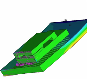
Figure 1. Finite element computer model of circuit board with microchip. |
Electronic components are being used in increasingly more abusive environments. This combined with an industry trend of increased component reliability to help reduce electronic system downtime has created an increasing demand for understanding the loads imparted through a printed circuit board to an individual component on the board such as a microchip. Local stiffening of the circuit board can limit the component loads, however stiffening devices can be costly to design and implement. They are also bulky, taking up valuable space on already crowded boards.
We used experimental and analytical tools to investigate how potentially damaging loads are transmitted through a circuit board to an individual component. We subjected a printed circuit board carrying a single microchip to impact loading. We adhered strain gages to the chip and the board and measured the level and duration of loads imparted to the board during normal handling, as well as some abuse.
We made a finite element computer model of the board and chip shown in Figure 1 to find out how much damage is caused to the chip from the abuse to the board. We predicted that even with abusive loading of the board, the only damage suffered by the chip would be to a small fraction of the chip connectors near its corners. The strain gage testing and finite element computer modeling proved invaluable; helping design the appropriate stiffening to mitigate the predicted damage
